- 您现在的位置:买卖IC网 > Sheet目录369 > W971GG6JB25I (Winbond Electronics)IC DDR2 SDRAM 1GBIT 84WBGA
�� �
�
�W971GG6JB�
�Notes:�
�1.� All� voltages� are� referenced� to� V� SS� .�
�2.� Tests� for� AC� timing,� I� DD� ,� and� electrical� AC� and� DC� characteristics� may� be� conducted� at� nominal� reference/supply� voltage�
�levels,� but� the� related� specifications� and� device� operation� are� guaranteed� for� the� full� voltage� range� specified.� ODT� is�
�disabled� for� all� measurements� that� are� not� ODT-specific.�
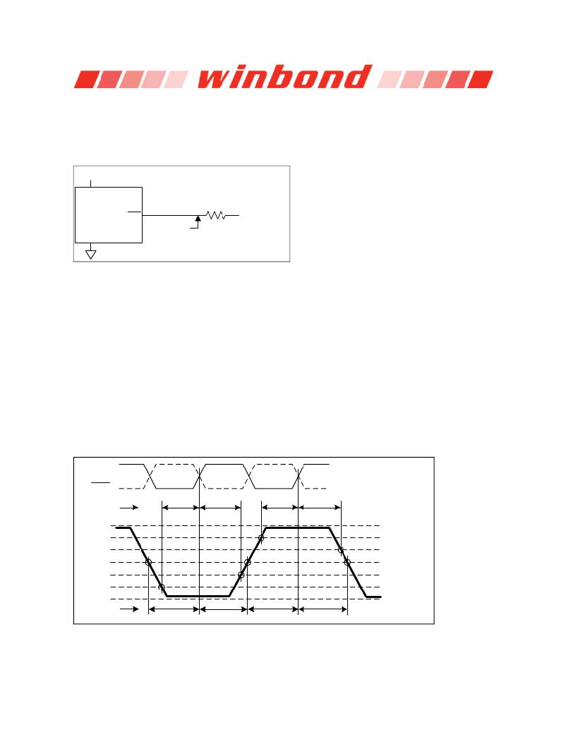
�3.� AC� timing� reference� load:�
�VDDQ�
�DQ�
�Output�
�DUT�
�DQS,� DQS�
�Figure� 16�
�Timing�
�25� Ω�
�reference�
�point�
�–� AC� timing� reference� load�
�VTT� =� VDDQ/2�
�4.� This� is� a� minimum� requirement.� Minimum� read� to� precharge� timing� is� AL� +� BL� /� 2� provided� that� the� tRTP� and� tRAS(min)�
�have� been� satisfied.�
�5.� If� refresh� timing� is� violated,� data� corruption� may� occur� and� the� data� must� be� re-written� with� valid� data� before� a� valid� READ�
�can� be� executed.�
�6.� This� is� an� optional� feature.� For� detailed� information,� please� refer� to� “� Operating� Temperature� Condition� ”� section� 10.2� in�
�this� data� sheet.�
�7.� tCKE� min� of� 3� clocks� means� CKE� must� be� registered� on� three� consecutive� positive� clock� edges.� CKE� must� remain� at� the�
�valid� input� level� the� entire� time� it� takes� to� achieve� the� 3� clocks� of� registration.� Thus,� after� any� CKE� transition,� CKE� may� not�
�transition� from� its� valid� level� during� the� time� period� of� tIS� +� 2� x� tCK� +� tIH.�
�8.� A� minimum� of� two� clocks� (2� *� nCK)� is� required� irrespective� of� operating� frequency.�
�9.� tWTR� is� at� least� two� clocks� (2� *� nCK)� independent� of� operation� frequency.�
�10.� There� are� two� sets� of� values� listed� for� Command/Address� input� setup� time:� tIS(base)� and� tIS(ref).� The� tIS(ref)� value� (for�
�reference� only)� is� equivalent� to� the� baseline� value� of� tIS(base)� at� VREF� when� the� slew� rate� is� 1.0� V/nS.� The� baseline� value�
�tIS(base)� is� the� JEDEC� defined� value,� referenced� from� the� input� signal� crossing� at� the� VIH(ac)� level� for� a� rising� signal� and�
�VIL(ac)� for� a� falling� signal� applied� to� the� device� under� test.� See� Figure� 17.� If� the� Command/Address� slew� rate� is� not� equal� to�
�1.0� V/nS,� then� the� baseline� values� must� be� derated� by� adding� the� values� from� table� of� tIS/tIH� derating� values� for� DDR2-667,�
�DDR2-800� and� DDR2-1066� (page� 55).�
�CLK�
�CLK�
�t� IS(base)� t� IH(base)�
�t� IS(base)� t� IH(base)�
�Logic� levels�
�V� DDQ�
�V� IH(ac)� min�
�V� IH(dc)� min�
�V� REF(dc)�
�V� IL(dc)� max�
�V� IL(ac)� max�
�V� SS�
�V� REF� levels�
�t� IS(ref)�
�t� IH(ref)�
�t� IS(ref)�
�t� IH(ref)�
�Figure� 17�
�–� Differential� input� waveform� timing� –� tIS� and� tIH�
�Publication� Release� Date:� Sep.� 24,� 2013�
�-� 47� -�
�Revision� A09�
�发布紧急采购,3分钟左右您将得到回复。
相关PDF资料
W971GG8JB-25
IC DDR2 SDRAM 1GBIT 60WBGA
W9725G6IB-25
IC DDR2-800 SDRAM 256MB 84-WBGA
W9725G6JB25I
IC DDR2 SDRAM 256MBIT 84WBGA
W9725G6KB-25I
IC DDR2 SDRAM 256MBIT 84WBGA
W972GG6JB-3I
IC DDR2 SDRAM 2GBITS 84WBGA
W9751G6IB-25
IC DDR2-800 SDRAM 512MB 84-WBGA
W9751G6KB-25
IC DDR2 SDRAM 512MBIT 84WBGA
W9812G6JH-6I
IC SDRAM 128MBIT 54TSOPII
相关代理商/技术参数
W971GG6JB-25I
制造商:Winbond Electronics 功能描述:-40~85 1GB DDR2 FOR INDUSTRY
W971GG6JB25ITR
制造商:Winbond Electronics Corp 功能描述:1G, DDR2-800, X16, IND TEMP
W971GG6JB25TR
制造商:Winbond Electronics Corp 功能描述:NR, DDR2-800, X16
W971GG6JB-3
制造商:Winbond Electronics Corp 功能描述:1GBIT DDRII
W971GG6KB-18
制造商:Winbond Electronics Corp 功能描述:1G, DDR2-1066, X16 制造商:Winbond Electronics Corp 功能描述:IC MEMORY
W971GG8JB
制造商:WINBOND 制造商全称:Winbond 功能描述:16M × 8 BANKS × 8 BIT DDR2 SDRAM
W971GG8JB-25
功能描述:IC DDR2 SDRAM 1GBIT 60WBGA RoHS:是 类别:集成电路 (IC) >> 存储器 系列:- 标准包装:72 系列:- 格式 - 存储器:RAM 存储器类型:SRAM - 同步 存储容量:4.5M(256K x 18) 速度:133MHz 接口:并联 电源电压:3.135 V ~ 3.465 V 工作温度:0°C ~ 70°C 封装/外壳:100-LQFP 供应商设备封装:100-TQFP(14x20) 包装:托盘
W9725G6IB-25
功能描述:IC DDR2-800 SDRAM 256MB 84-WBGA RoHS:是 类别:集成电路 (IC) >> 存储器 系列:- 标准包装:1,000 系列:- 格式 - 存储器:EEPROMs - 串行 存储器类型:EEPROM 存储容量:4K (512 x 8) 速度:400kHz 接口:I²C,2 线串口 电源电压:2.7 V ~ 5.5 V 工作温度:-40°C ~ 85°C 封装/外壳:8-SOIC(0.173",4.40mm 宽) 供应商设备封装:8-MFP 包装:带卷 (TR)